current position: Home > News > News > Common problem
Common Hu detection methods and experience sharing in the use of field effect tubes
The resistance measurement method is to use a multimeter to measure the resistance value between the source and drain, the gate and the source, the gate and the drain, the gate G1 and the gate G2 of the field effect tube, and the resistance value indicated in the field effect tube manual Whether it matches to judge the quality of the tube.
Specific test method of field effect tube:
one. Place the multimeter in the R×10 or R×100 gear, and measure the resistance between the source S and the drain D, usually in the range of tens of ohms to several thousand ohms.
2. The measured resistance is greater than the normal value, which may be due to poor internal contact; if the measured resistance is infinite, it may be an internal disconnection. Then set the multimeter to the R×10k file, and then measure the resistance between the gate G1 and G2, between the gate and the source, and between the gate and the drain.
3. All resistance values are infinite, indicating that the tube is normal; if the above resistance values are measured to be too small or a path, it means that the tube is broken.
4. Special attention should be paid to the fact that if the two grids are broken in the tube, the component substitution method can be used for detection.

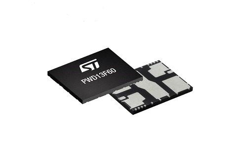
Figure 1: ST's SiP solution for industrial motor drivers, lamp ballasts, power supplies, converters and inverter applications
The shutdown circuit can protect the power switch, and the under-voltage lockout can prevent low-voltage faults. Similarly, the bootstrap diode can reduce the bill of materials (BOM) and simplify the circuit board layout.
It shows why packaging options are critical to maximizing energy efficiency and adapting to a wide range of supply voltages. Here, it is also worth pointing out that the power density of the package and the improvement of heat dissipation conditions complement each other.
3. Heat dissipation efficiency
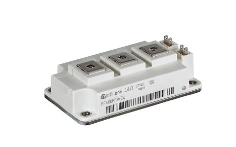
Since devices such as IGBTs work at lower temperatures to reduce the stress on the devices, the heat dissipation performance of the package is inherently related to its reliability (Figure 2). Since the size of the heat sink required for a lower temperature is not large, the heat dissipation characteristics will also affect the size of the heat sink. In addition, the reduction in cooling requirements also leaves more room for designers to increase power density.

Figure 2: Infineon’s power module package uses thermal interface material (TIM)
Some packages retain the size of the package and the bottom design with high heat dissipation efficiency, while leaving the top source exposed as a heat dissipation area. This can achieve a higher rated current value, thereby achieving a higher power density and a smaller package size.
4. Heat dissipation
Conventional methods for creating isolation inside the package are often expensive and difficult to handle. Moreover, they are far from sufficient to manage the heat dissipation of high power density devices such as IGBTs.
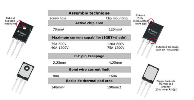
Therefore, Infineon introduced a packaging technology called Trenchstop advanced isolation (Figure 3). The German chip manufacturer claims that Trenchstop packaging technology can replace FullPAK and standard isolation foils. Infineon positions this new package in applications such as power factor correction (PFC), uninterruptible power supply (UPS) and power converters for air conditioners.

Figure 3: The heat generated by the package on the right is reduced by 15%
This isolation package no longer requires isolation materials and thermal grease, allowing designers to reduce assembly time by up to 35%. At the same time, because there is no misalignment of the isolation foil, it also improves reliability. This also achieves an improvement that is 10°C lower than the operating temperature of FullPAK.
5. Switching loss
Especially for hard-switching circuits with operating frequencies up to 20kHz in devices such as industrial drivers, it is imperative to reduce switching losses in order to improve packaging efficiency. In addition, reliable switching and low EMI enhance heat sink-less operation in low-power applications.
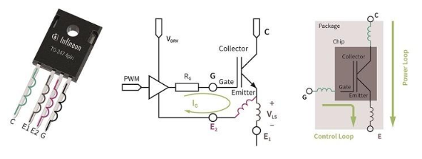
To reduce switching losses, some packaging solutions use additional Kelvin emitter power pins (Figure 4). It bypasses the emitter lead inductance of the gate control loop, thereby increasing the switching speed of the device and reducing the switching energy.

Figure 4: A package with a Kelvin emitter can reduce dynamic losses by 20%.
This article tags:What,are,the,key,factors,that,need,considered,for,packaging The last:About IGBT tube detection shar The last:What are the common FETs?Tel: 0755-83948880
Fax: 0755-83948881
E-mail: sales@sunshineic.com
Add: RM 603, Building 405, Shangbu Industrial Area, Zhenxing RD, Futian District , Shenzhen, China
 Wechat QR code
 Phone QR code